- 您现在的位置:买卖IC网 > Sheet目录395 > AT86RF231-ZFR (Atmel)TXRX LOW POWER 2.4GHZ 32VQFN
AT86RF231
1.2
1.2.1
1.2.2
Analog and RF Pins
Supply and Ground Pins
EVDD, DEVDD
EVDD and DEVDD are analog and digital supply voltage pins of the AT86RF231 radio
transceiver.
AVDD, DVDD
AVDD and DVDD are outputs of the internal 1.8V voltage regulators. The voltage regulators are
controlled independently by the radio transceivers state machine and are activated dependent
on the current radio transceiver state. The voltage regulators can be configured for external
supply.
For details, refer to Section 9.4 “Voltage Regulators (AVREG, DVREG)” on page 110 .
AVSS, DVSS
AVSS and DVSS are analog and digital ground pins respectively. The analog and digital power
domains should be separated on the PCB.
RF Pins
RFN, RFP
A differential RF port (RFP/RFN) provides common-mode rejection to suppress the switching
noise of the internal digital signal processing blocks. At board-level, the differential RF layout
ensures high receiver sensitivity by rejecting any spurious emissions originated from other digital
ICs such as a microcontroller.
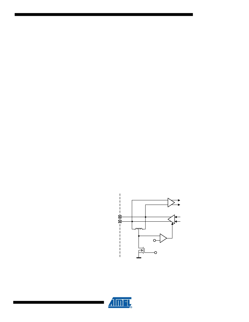
A simplified schematic of the RF front end is shown in Figure 1-2 on page 5 .
Figure 1-2.
Simplified RF Front-end Schematic
PCB
AT86RF231
LNA
RX
RFP
RFN
M0
0.9V
RXTX
PA
CM
Feedback
TX
The RF port is designed for a 100 Ω differential load. A DC path between the RF pins is allowed.
A DC path to ground or supply voltage is not allowed. Therefore, when connecting an RF-load
providing a DC path to the power supply or ground, AC-coupling is required as indicated in Table
1-2 on page 6 .
5
8111C–MCU Wireless–09/09
发布紧急采购,3分钟左右您将得到回复。
相关PDF资料
AT86RF232-ZX
2.4 GHZ ZIGBEE TRANSCEIVER
AT88CK201BK
BRD CRYPTORF READER AT88RF1354
AT88SC-ADK2
KIT ARIS+ DK CRYPTOMEM/COMPANION
AT88SC3216CRF-MY1
IC EEPROM 32KBIT 13MHZ TAG
ATA-2001
LVDT AMPLIFIER
ATAB5429-9-B
BOARD BASESTATN UHF RCVR 915MHZ
ATAB5749-3
BOARD XMITTER FOR 315MHZ ATA5749
ATAKSTK511-3
KIT RF MODULE 315MHZ FOR STK500
相关代理商/技术参数
AT86RF231-ZU
功能描述:射频收发器 2.4GHz Zigbee Transceiver
RoHS:否 制造商:Atmel 频率范围:2322 MHz to 2527 MHz 最大数据速率:2000 Kbps 调制格式:OQPSK 输出功率:4 dBm 类型: 工作电源电压:1.8 V to 3.6 V 最大工作温度:+ 85 C 接口类型:SPI 封装 / 箱体:QFN-32 封装:Tray
AT86RF231-ZU_09
制造商:ATMEL 制造商全称:ATMEL Corporation 功能描述:Low Power 2.4 GHz Transceiver for ZigBee
AT86RF231-ZUR
功能描述:射频收发器 2.4GHz, Zigbee Transceiver
RoHS:否 制造商:Atmel 频率范围:2322 MHz to 2527 MHz 最大数据速率:2000 Kbps 调制格式:OQPSK 输出功率:4 dBm 类型: 工作电源电压:1.8 V to 3.6 V 最大工作温度:+ 85 C 接口类型:SPI 封装 / 箱体:QFN-32 封装:Tray
AT86RF232-ZX
功能描述:射频收发器 2.4 GHZ ZIGBEE TRANSCEIVER
RoHS:否 制造商:Atmel 频率范围:2322 MHz to 2527 MHz 最大数据速率:2000 Kbps 调制格式:OQPSK 输出功率:4 dBm 类型: 工作电源电压:1.8 V to 3.6 V 最大工作温度:+ 85 C 接口类型:SPI 封装 / 箱体:QFN-32 封装:Tray
AT86RF232-ZXR
功能描述:射频收发器 2.4 GHZ ZIGBEE TRANSCEIVER
RoHS:否 制造商:Atmel 频率范围:2322 MHz to 2527 MHz 最大数据速率:2000 Kbps 调制格式:OQPSK 输出功率:4 dBm 类型: 工作电源电压:1.8 V to 3.6 V 最大工作温度:+ 85 C 接口类型:SPI 封装 / 箱体:QFN-32 封装:Tray
AT86RF233-ZF
功能描述:IC RF TXRX+MCU 802.15.4 32-VFQFN 制造商:microchip technology 系列:- 包装:托盘 零件状态:在售 类型:TxRx + MCU 射频系列/标准:802.15.4,通用 ISM > 1GHz 协议:6LoWPAN,Zigbee? 调制:O-QPSK 频率:2.4GHz 数据速率(最大值):2Mbps 功率 - 输出:4dBm 灵敏度:-101dBm 存储容量:128B SRAM 串行接口:SPI 电压 - 电源:1.8 V ~ 3.6 V 电流 - 接收:11.3mA ~ 11.8mA 电流 - 传输:7.2mA ~ 13.8mA 工作温度:-40°C ~ 125°C 封装/外壳:32-VFQFN 裸露焊盘 标准包装:490
AT86RF233-ZFR
功能描述:IC RF TXRX+MCU 802.15.4 32-VFQFN 制造商:microchip technology 系列:- 包装:剪切带(CT) 零件状态:在售 类型:TxRx + MCU 射频系列/标准:802.15.4,通用 ISM > 1GHz 协议:6LoWPAN,Zigbee? 调制:O-QPSK 频率:2.4GHz 数据速率(最大值):2Mbps 功率 - 输出:4dBm 灵敏度:-101dBm 存储容量:128B SRAM 串行接口:SPI 电压 - 电源:1.8 V ~ 3.6 V 电流 - 接收:11.3mA ~ 11.8mA 电流 - 传输:7.2mA ~ 13.8mA 工作温度:-40°C ~ 125°C 封装/外壳:32-VFQFN 裸露焊盘 标准包装:1
AT86RF233-ZU
功能描述:射频收发器 2.4GHz ZigBee Transceiver
RoHS:否 制造商:Atmel 频率范围:2322 MHz to 2527 MHz 最大数据速率:2000 Kbps 调制格式:OQPSK 输出功率:4 dBm 类型: 工作电源电压:1.8 V to 3.6 V 最大工作温度:+ 85 C 接口类型:SPI 封装 / 箱体:QFN-32 封装:Tray
